

Ultrasonic Cleaning in Semiconductor Manufacturing Industry
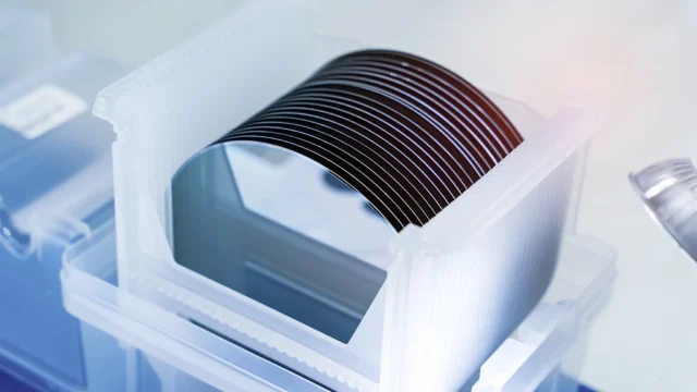
In semiconductor manufacturing, precision is crucial. Nanoscale imperfections can disrupt electronic devices, making cleanliness mission-critical. Among the array of techniques employed to achieve pristine surfaces, ultrasonic cleaning stands out as a powerful and versatile solution. We will further delve into the applications of ultrasonic cleaning in semiconductor manufacturing.
Why is ultrasonic cleaning important for semiconductors?
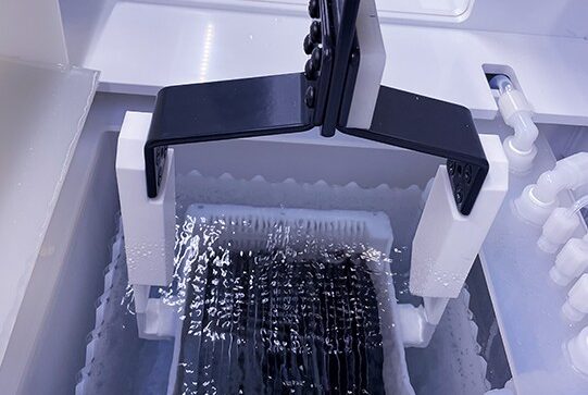
Ultrasonic cleaning plays a vital role in the semiconductor manufacturing industry due to its ability to effectively remove contaminants from delicate and intricate components. Semiconductor devices are highly sensitive and require stringent cleanliness standards to ensure optimal performance and reliability. Here are some reasons why ultrasonic cleaning is essential in semiconductor manufacturing:
-
- Superior cleaning efficacy
Removes even the most stubborn contaminants, such as organic residues, metal particles, and polishing compounds.
- Superior cleaning efficacy
-
- Gentle on delicate surfaces
Unlike mechanical scrubbing, ultrasonic cleaning does not cause scratches or damage to sensitive semiconductor structures.
- Gentle on delicate surfaces
-
- Reaches hidden areas
Effectively cleans blind holes, trenches, and other complex geometries.
- Reaches hidden areas
-
- Improves process yields
Minimizes device failure due to contamination, leading to higher production yields.
- Improves process yields
-
- Reduces chemical usage
Often requires less cleaning chemicals compared to traditional methods.
- Reduces chemical usage
Semiconductor manufacturing plays a pivotal role in the production of mobile phones, serving as the foundation for the intricate electronic components that power these devices. The process involves creating semiconductor wafers through intricate steps such as photolithography, deposition, and etching. Wafers are diced into chips, serving specific functions like processors, memory, and sensors.
Beyond Wafer Cleaning
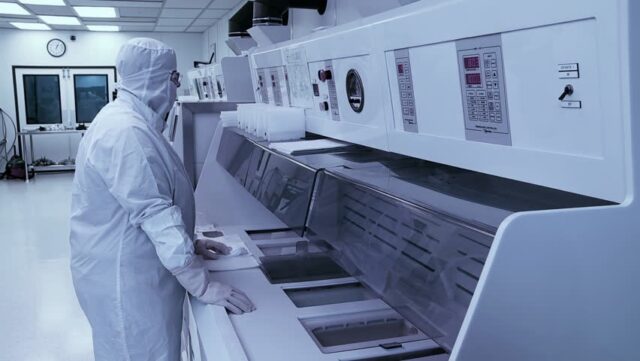
Although wafer cleaning is the main purpose, ultrasonic cleaning has several other applications in the semiconductor production process. To avoid cross-contamination and preserve process integrity, it is used to clean tools and equipment like etching reactors and deposition chambers. Furthermore, to guarantee the cleanliness of vital components like leads and bond pads, ultrasonic cleaning is essential at the last device packing stage.
-
- Tool and Equipment Maintenance
Tools and equipment used in semiconductor production, including as etching systems and deposition chambers, are essential to the fabrication process. Constant operation may cause impurities to build up and could lower the quality of the devices that are created. Because ultrasonic cleaning enables in-situ cleaning without requiring disassembly, it provides a solution that is not just efficient but also reduces downtime.
- Tool and Equipment Maintenance
-
- Precision Part Cleansing
Ultrasonic cleaning can achieve the level of cleanliness required by numerous precision parts and components in the complex dance of semiconductor manufacture. Because of their intricate designs and small areas, nozzles, valves, and chambers benefit from the accuracy of ultrasonic cleaning, which guarantees that every nook and cranny is clear of impurities.
- Precision Part Cleansing
-
- Critical Component Care
Reticles and photomasks, which are necessary for the photolithography process, must be handled carefully. These vital components can be kept clean and intact with the use of ultrasonic cleaning, which helps to achieve the excellent patterning needed for semiconductor manufacture.
- Critical Component Care
-
- Advanced Packaging
Ultrasonic cleaning has become a viable method for guaranteeing the dependability of packaged devices as semiconductor packaging techniques progress. Ultrasonic cleaning eliminates impurities and flux residues in solder joints critical to operations like flip-chip bonding, enabling strong and reliable electronic packages.
- Advanced Packaging
The Future of Ultrasonic Cleaning in Semiconductors
As transistors shrink, ultrasonic technology evolves. Nanoscale cleaning is becoming possible because of developments in ultrasonic technology, including concentrated cavitation and the use of higher frequencies. Ensuring the continuous development of increasingly compact and potent semiconductor devices will depend on this.
Conclusion: The Microscopic World of Ultrasonic Cleaning in the Semiconductor Industry
An essential tool in the high-stakes world of semiconductor manufacture is ultrasonic cleaning. The quality, dependability, and functionality of these vital parts depend heavily on their capacity to precisely and effectively eliminate minute impurities. Ultrasonic cleaning technology will surely continue to develop as the industry pushes the limits of downsizing, making a significant contribution to the future of electronics.
